Blog
Key Trends Shaping the Future of Printed Circuit Boards
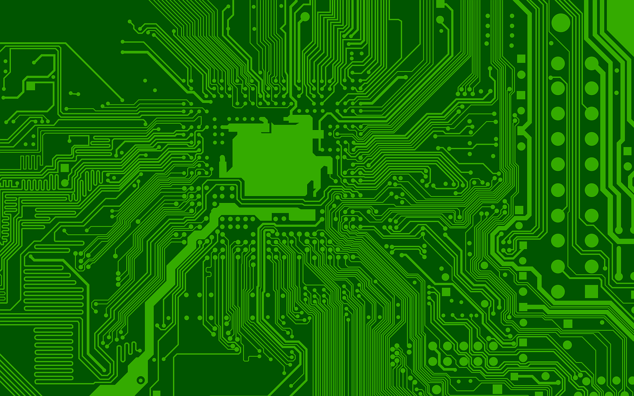
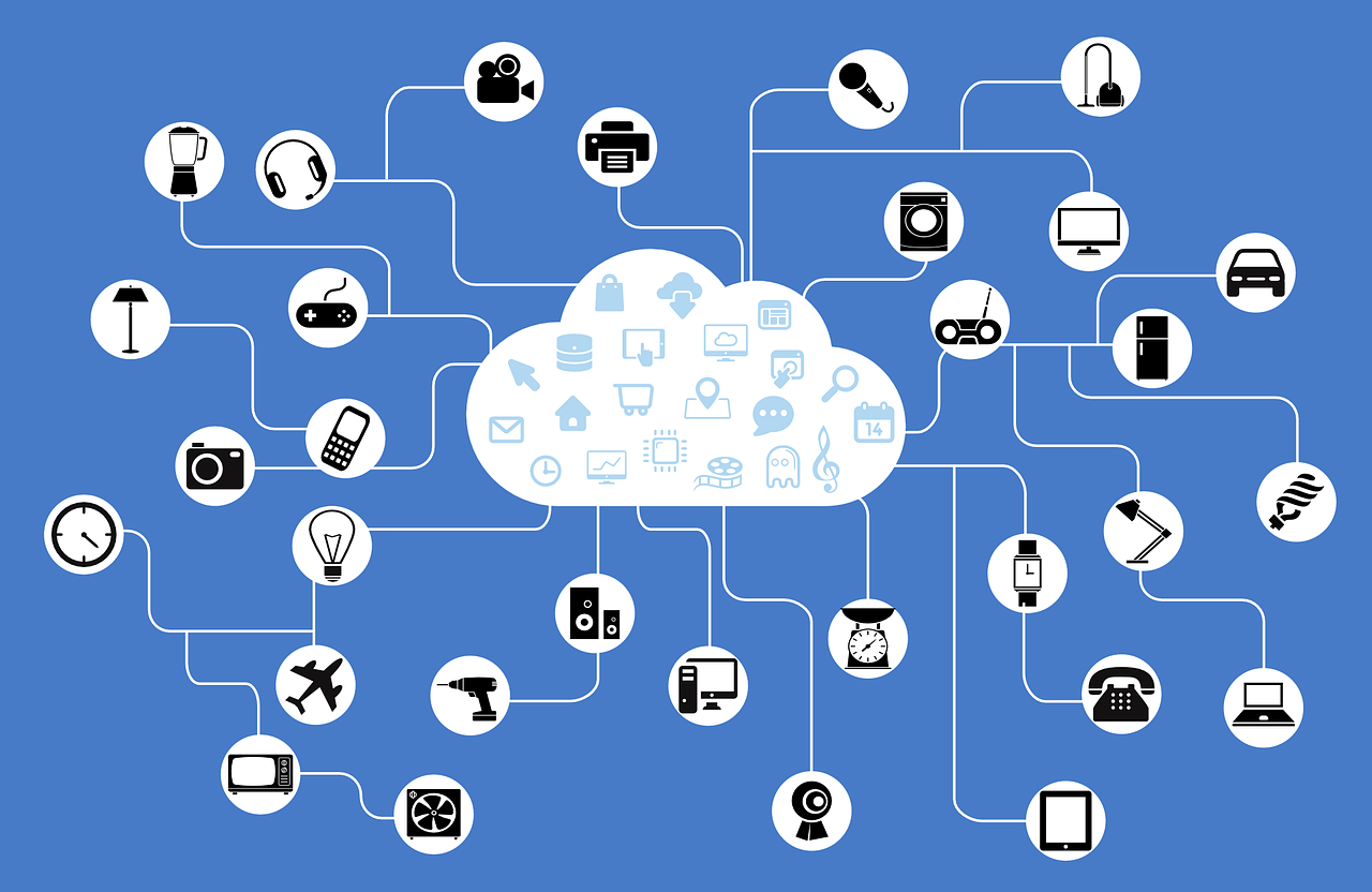
Innovations and an increase in demand for more compact and powerful electronic devices continue to become a main factor that drives growth and evolves the use of printed circuit boards. Printed Circuit Boards (PCBs) are continuously evolving and are driven by tech advancements and changing market demands. To stay ahead of this competitive landscape, you must understand the key trends shaping PCBs' future. In this article, we’ll learn more about them and how they are evolving electronic products. Key trends driven by technological advancements shape circuit boards' future, the demand for more efficient electric devices, and achieving a more sustainable environment. The demand for smaller and more powerful electronics will keep growing, and PCBs need to be designed to accommodate more components and take up less space. HDI technology allows the miniaturization of PCBs via multilayered boards that include fine-pitch components. This technology can be used to bring innovations to a range of industries. The main goal here is to make sure that circuit boards have higher component density. HDI achieves this through advanced techniques that allow it to achieve higher performance and density. Fine-line microvia technology is a part of HDI techniques and is used for achieving this. Electronics are getting much smaller over the years, requiring smaller component pitches than before. First-line microvia technology makes this possible. It is a drilled and plated hole that creates interconnections between copper layers of a PCB. Micro-vias are used for creating more space in a given design or when using fine-pitch components. AI has made significant changes to every industry in the world. 35% of all global companies are using AI in their business. Imagine that nearly half of the companies in the world are starting to use AI in their everyday operations. This means that AI is already playing a significant role in many industries, including PCB manufacturing and assembly. Moreover, Machine Learning (ML) algorithms improve quality control and identify any issues during the production phase. The power of AI even helps inspection systems detect the smallest imperfections, making sure that the PCM assembly is at its highest quality. The help of AI can also be used during the design phase, helping engineers improve PCB manufacturing and assembly performance, how heat is dissipated, and signal integrity. The AI helps in allowing more accurate and faster prototyping, reducing new product's time-to-market. Moreover, let’s not forget that AI is also capable of analyzing data and real-time information, which is helpful in finding faults and root causes in the manufacturing process. Additive manufacturing includes joining materials layer upon layer to make them from 3D model data (3D printing) and is a choice used compared to low-volume product or PCB prototyping. The advantage 3D-printed PCBs have is that they have many customizable options and reduce lead times. It may not be used for mass production, but can accelerate prototyping compared to subtractive manufacturing. Considering this, soon, the demand for 3D-printed circuit boards is most likely going to increase. 3D printing involves depositing material under software control. The most commonly used materials include powder grains and liquids. These are all added layer by layer and help in reducing costs, increasing production speed, and customization in PCB manufacturing. It’s becoming a popular method since it prints the substrate one layer at a time by initially adding liquid ink, and right after, adding the needed surface-mounted components. 3D printing can significantly reduce waste, which means that it’s a cost-effective option and better for the environment. The more complex a design is, the more useful 3D printing becomes for you. There’s only one challenge involved with 3D printing for PCBs, and that is reducing resolution. The current limit is a width of a micron, but it needs to get down to the micron level to compete with the best available techniques out there. However, for this challenge, you can solve the problem by using a self-assembly or adopting a photolithography. Integrating the Internet of Things (IoT) in PCB tech is greatly transforming the industry in 2023. It helps in increasing operational efficiency through automation. IoT collects devices that use processing and sensor capabilities to exchange data with devices over a given network. IoT-based approaches use multiple layers of high-speed connectivity, more commonly for wireless networks. Something to keep in mind is that PCBs for IoT devices need to meet more requirements compared to those of regular PCBs. However, the positive side is that manufacturers can fabricate wireless PCBs quickly. Almost all industries benefit from IoT and companies will use this type of technology for controlling and monitoring devices from home and workplace remotely. Industries that benefit the most from IoT integration include: Wearable technologies Industrial automation Healthcare Manufacturing Transportation and logistics The use of IoT devices is driving the need for circuit boards that support low power consumption and wireless communication. There are plenty of materials that are considered advanced. Many more electronic devices are now requiring PCBs to be manufactured using materials that possess different characteristics than the ones that were traditionally used. Here is a list of advanced materials that are being used to meet these requirements: Ceramic substrates: Offer great thermal management, improving how PCBs transfer heat from hot spots and offer better heat dissipation. Ceramic substrates are an important material that is used in many industries, specifically in aerospace, electronics, automotive, and more. Electric devices need efficient thermal management, so ceramic substrates make this possible. High frequency laminates with stable dielectric constant: Helps in improving reliability and reduces signal losses. This material is mostly popular in the medical and defense industries since they need to have strong signals at all times. Flex substrate and rigid-flexible PCBs: This includes boards that have multiple layers that are attached to one or more rigid boards. They are a great fit for applications that require the PCB to be curved to fit in unusual shapes and sizes to perform flawlessly in extreme climates (i.e. high temperatures). Flexible PCBs are used in mobile phones, desktops, tablets, and more. Biodegradable polymers: Are used to replace toxic thermosetting resins that are used in PCB manufacturing. However, keep in mind that this material can’t withstand chemical washes or etching, so this is something to note. Advanced materials are changing the way PCB manufacturing and assembling is done. Not only is it preparing electric devices to withstand more extreme temperature environments, but advanced materials are increasing reliability and reducing signal losses. Electric devices have undergone a significant transformation over the past few years, increasing functionality and complexity. The manufacturing of circuit boards involves materials that raise environmental concerns. Research shows that 6.7 PCBs make up roughly 42% of total e-waste weight. Conventional boards, on the other hand, utilize materials like fiberglass reinforced with epoxy resin, which makes it challenging to recycle and dispose of because of their non-biodegradable nature. The solutions to environmental challenges include green circuit boards, which are used for sustainable practices in electronics and seek to reduce environmental impacts made by electronic devices by deploying recyclable materials and eco-friendly manufacturing practices. Green circuit boards are great for the environment since they offer materials like bioplastics, recycled paper, and bamboo-derived substrates. These types of materials are easily recyclable, which means that there is less harm to the environment from electronic devices. Using eco-friendly circuit boards has a positive impact on the environment, reducing environmental impact, offering much better thermal management, and reducing unnecessary energy consumption. Let’s not forget that manufacturers are also obliged to comply with the Restriction of Hazardous Substances (RoHS) since it restricts using materials like mercury, lead, and cadmium. The future of the PCB industry is going to be shaped by an increase in demand for an interconnected and tech-driven world. Advancements in technology and materials that are used in PCB manufacturing and assembly will help shape your future of products in terms of reliability and sustainability. Key trends are what highlight the dynamic nature of circuit boards that are driven by technological advancements, marketing demands, and the demand for a more sustainable environment. 6 Trends shaping the future of Printed Circuit Boards (PCB)
Miniaturization and high-density interconnect (HDI) to create more space in a given design
Artificial Intelligence (AI) for improving the PCB manufacturing and assembly phase
Additive manufacturing and 3D printing
IoT integration
The use of advanced materials
Material eco-friendly innovations
PCB trends are shaping its future
About The Author:
Tony Ademi is a freelance SEO content and copywriter. He has been in the writing industry for three years and has managed to write hundreds of SEO-optimized articles. Moreover, he has written articles that have ranked #1 on Google. Tony’s primary concern when writing an article is to do extensive research and ensure that the reader is engaged until the end.